A Flash Translation Layer (FTL) is responsible for abstracting away the details of internal SSD architecture and characteristics from the host OS. While the Flash Drive (or Solid-State Drive, SSD) has many advantages over Hard Disk Drive (HDD), more operation characteristics are raised and waiting to be handled. For example, Flash Drive can perform read and write on page level but can only perform erase on the block level. Meanwhile, every block has an erase limit, so FTL must have leveling algorithm to ensure every block can be erased evenly.
To make design and implementation more specified, the following constraints are applied:
The major design choices on FLT are the mapping strategy, garbage collection, and wear-leveling strategy.
In checkpoint1 and 2 of this project, we were taught to implement a block-level mapping scheme in our FTL. While the data layout is straightforward, it has significant write amplification and is not an optimal choice for the endurance of our SSD.
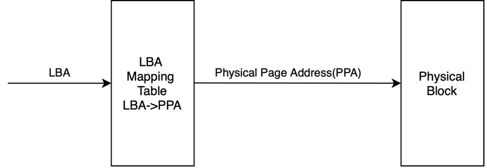
To maximize the endurance and minimize the write amplification, the page-level mapping scheme is used in checkpoint3. The translation process of our FTL is as follows:

Using the LBA Mapping Table, we can map any LBA address to any PPA address and enhance the flexibility of future operations (i.e., garbage collection and wear-leveling).
Because of the Flash Device’s properties, we cannot perform page-level erase. When a write is issued to a valid LBA (contains valid data in it), we simply invalidate the original physical page and write new data to a new physical page. This will inevitably cause fragmentation on Flash. When overprovisioned space is used up, we must clean the fragmentations to free more space for writers. This is called garbage collection.
Meanwhile, each block has limited erases. Once a block exceeds its designed erases, it will become unreliable and not functional. Making sure the blocks are erased evenly is another design choice for the FTL.